A recent survey conducted by Keithley Instruments, Inc. of participants in the solar cell/photovoltaic device industry indicates distinct differences in testing methods and priorities among respondents from Asia, North America, and Europe. The study included responses from solar cell/photovoltaic device researchers and manufacturers working in government, university-based, and corporate labs and manufacturing facilities around the world.
The survey asked respondents whether they were involved in early stage research, product development activity, or full scale production of solar cell/PV devices. As would be expected, different test priorities emerged not only geographically, but among those testing devices at early stages compared to production testing.
In addition, the survey queried respondents about various device technologies they were testing. Overall, the survey showed more R&D activity in thin film materials over silicon-based devices, regardless of geography. And among those with devices currently in production, there was no discernable difference in test methodologies between those currently producing thin film-based devices vs. silicon.
Finally, across all geographies, the survey showed the industry is focused on improving device efficiencies as the dominant development priority. "Reducing manufacturing cost" was the second most important among the respondents, as might be expected, although substantially less significant than the need to boost device and panel performance.
Current Activity Remains Focused on Research
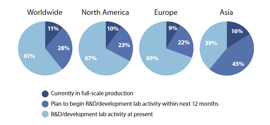
The vast majority of respondents to the survey noted that they were presently involved in early stage R&D/development lab activity, although Asian respondents noted they were farther down the development path to full-scale production. Overall, 61% of overall respondents reported they were in the R&D lab stage, compared to 67% for North America and just 39% for Asia.Similarly, those in full-scale production represented 11% of the survey respondents, compared to 10% in North America and 16% in Asia. European responses were similar to those from North America.
Clear Priority Emerges for Top Four Solar Cell Test Methods
For those engaged in solar cell research and development, a large majority of respondents worldwide identified their "key parameters" for measurement as short-circuit current (ISC), open-circuit voltage (VOC), maximum output power (PMAX) and, to a lesser extent, conversion efficiency. Respondents in North America and Europe showed consistent agreement on what constitutes their most important tests, with a well-defined gap between these top four and 10 other tests. Respondents from Asia, while agreeing with the same top four tests, showed much less preference for them as other tests were cited as key parameters nearly as often as the top four. (Refer to the "Solar Cell Testing Glossary" at the end of this white paper for details on the various test types/parameters.)
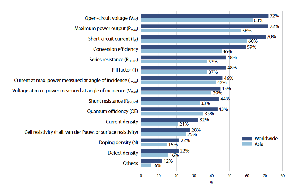
"The top three tests indicated by respondents are consistent with what customers tell us are important methodologies for them in the research phase," noted Keithley Marketing Director Mark Cejer. "Those tests in particular are focused on improving efficiency of the device and are used by most as the core of electrical test methods on solar cell devices. We were a bit surprised not to see more priority given to shunt resistance and series resistance tests, as we hear quite a bit about how important those measurements are to characterizing device performance. Overall, other than a clear preference for the top three tests, there remains a significant amount of variation in the industry about what tests are most meaningful."
The priority of test parameters characterized as solar cell/photovoltaics move into production remained much the same, but there was far less agreement about the most important tests than was found in the research lab. And, Asian respondents were far more definitive about the most valuable solar cell tests for production than for research applications.
"Overall scores for production test actually reflected the common pattern of lowering overall production costs by reducing the level of test performed," said Cejer. "This was particularly true in North America when comparing research test levels to those in production test."
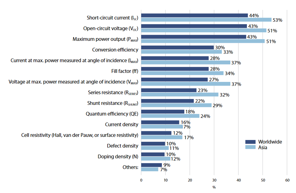
Engineers in general seem to be relatively unfazed by the solar cell industry's rather complicated battery of tests. When asked which tests presented technical challenges, none of the 15 tests appeared to pose a problem for a large portion of the respondents, either in the research or production test phase. This held true for even the most demanding tests included on the list, such as quantum efficiency and conversion efficiency. Maximum power output was identified as the most difficult test to perform, with 28% noting it as the "most challenging," perhaps reflecting the difficulty of integrating high power supplies and loads into a test system for this type of research.
PV Device Technologies
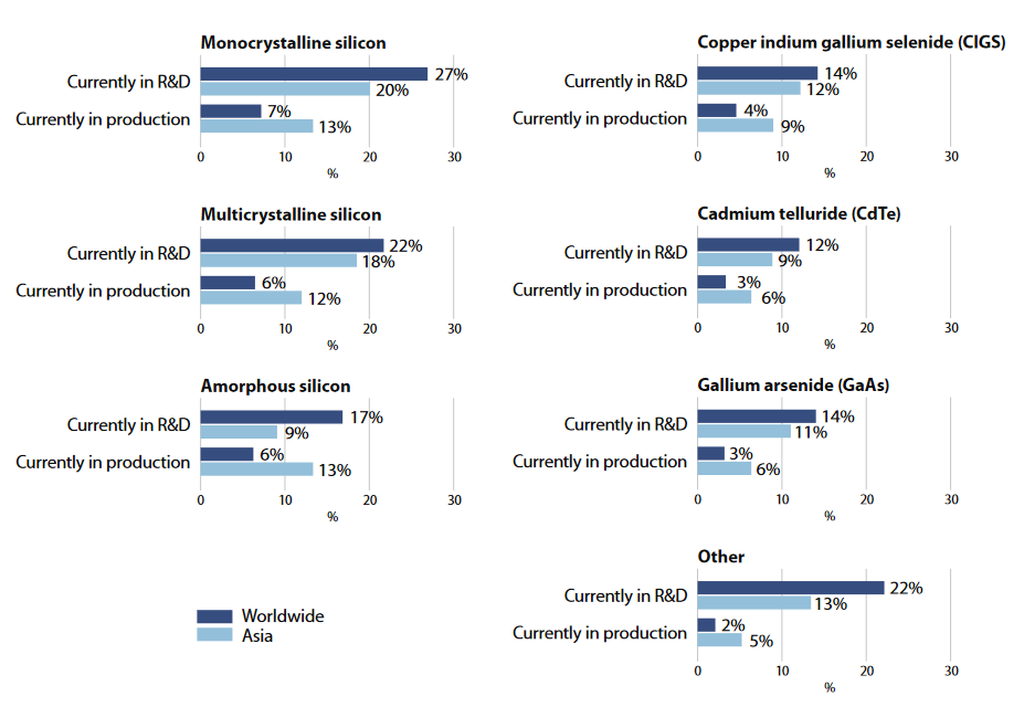
Survey respondents report engagement in a broad range of solar cell/PV device technologies, including established, relatively well-characterized technologies for making PV devices out of monocrystalline, multicrystalline, or amorphous silicon, as well as newer thin-film technologies such as copper indium gallium selenide (CIGS), cadmium telluride (CdTe), and gallium arsenide (GaAs). In general, respondents seemed more active in thin-film materials than in silicon, perhaps due to the cost advantages and greater efficiency of thin film technologies.
Not surprisingly, worldwide numbers of those reporting involvement in actual device production of thin-film technologies are lower, about half of current production levels for silicon-based solar cells.
However, almost one-third of respondents report involvement in materials and device research in far more exotic technologies, including nanotechnology-based materials, polymers, organics, dye-sensitized solar cells (DSSC), copper zinc tin sulfide (CZTS), gallium nitride (GaN), Cu2O/ZnO, silicon germanium tin, cadmium sulfide (CdS), cadmium selenide (CdSe), cadmium sulfide-cadmium telluride (CdS-CdTe), gallium selenide (GaSe), Grätzel cells, CuInGaSeTe, titanium oxide (TiO2), Sb:SnO2, copper oxide (CuO), cadmium oxide (CdO), InGaP/GaAs/Ge, photovoltaic inks, P3HT:PCBM, triple junction III-V cells, quantum dot solar cells, and many others.
End Uses of the PV Devices Being Produced
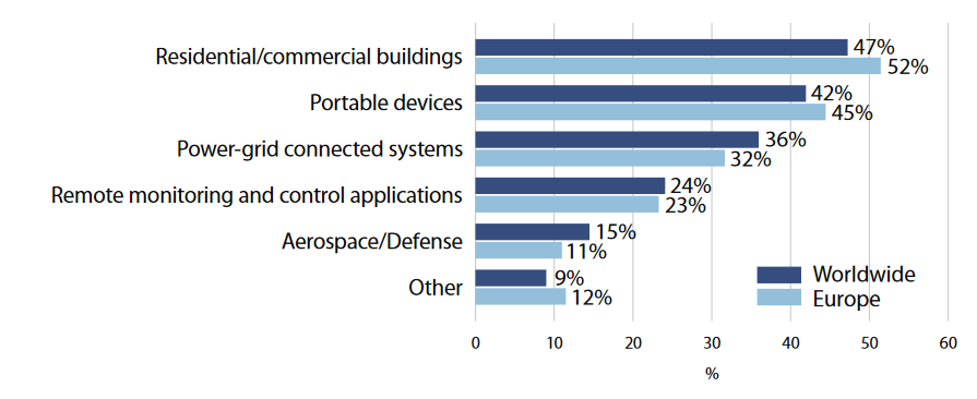
When asked to identify the end uses for their organization's products, the most commonly reported applications worldwide were in the areas of residential/commercial buildings and portable devices. Europe led the way in installations in residential/commercial buildings, likely due to Germany's and Italy's large installed base of solar cell panels.
Driving Down the Cost per Watt
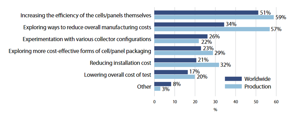
The industry seems focused on driving down costs of production and improving solar cell/PV efficiency. Respondents were asked how their organizations are working to reduce the cost per watt of the solar cells or panels they develop or manufacture. On a worldwide basis, more than half of all respondents report work on "increasing the efficiency of the cells/panels themselves," while roughly one-third cite "exploring ways to reduce overall manufacturing costs."
It's interesting to note that relatively few are concerned, at this early stage of the industry's life cycle, with lowering overall cost of test. Just 17% identified this as a priority, far lower than other initiatives. Certainly, as the industry matures, reducing cost of test will become a more pressing concern for engineers.
When responses from those currently in production are separated, the answers to this question indicate a different sense of urgency, one focused on improving operation efficiency. Those in production are far more concerned with finding ways to reduce overall manufacturing costs (57 percent compared to 34 percent for the overall group) and reducing installation cost (32 percent compared to 21 percent for the overall group).
Future Hiring Plans
When asked to forecast future hiring, nearly half of those responding worldwide report that they anticipate adding few or no staff members or full-time contractors to their work groups over the next year. The outlook for hiring in Asia, however, is considerably more optimistic than in the world as a whole, with 72% from that region anticipating their organizations will increase work group headcount by 5% or more. These hiring forecasts are in line with the Asian respondent's statements about gearing up for R&D within the next year.

The Future Points to Growth in Solar Cell Production
Although the percentage of those reporting engagement in full-scale production is relatively low today, the number of manufacturers seems destined to grow substantially over the next few years, with 43% reporting plans to move into full scale production in the next 12–36 months.
In Europe, EU mandates to increase the use of alternative energy sources and high energy costs will likely continue to drive investments in research there. In North America, the energy research and development portion of the U.S. economic stimulus bill (the American Recovery and Reinvestment Act of 2009) is likely to provide a boost to the nation’s solar industry. The situation in China is similar, in that the Chinese government included solar subsidies as part of its "green" stimulus package. These subsidies have the potential to improve the profitability of producing and selling solar cells for Chinese solar companies.
Given the staggering array of device technologies now being explored or developed, the industry seems poised to become larger and increasingly competitive, with manufacturers making significant investments in finding new ways to extract the maximum energy at the lowest possible cost from every photon that reaches their products. Asian manufacturers appear firmly committed to playing a major role in the worldwide solar cell industry.
Survey Demographics
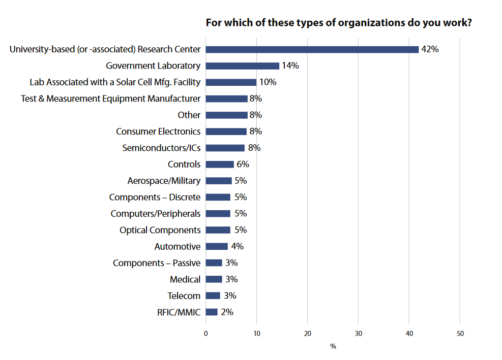
This survey was conducted in June 2009 by Keithley Instruments using a by-invitation-only online survey, generating 564 responses.
Solar Cell Testing Glossary
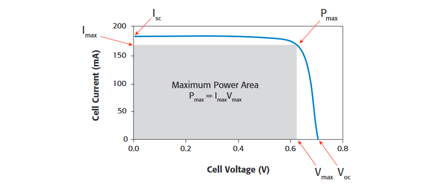
Short-circuit current (ISC): The point at which the I-V curve crosses the x axis at zero volts.When a solar cell is operated at short circuit (that is, when a low-resistance connection is established by accident or intention between two points in an electric circuit, so the current tends to flow through the area of low resistance, bypassing the rest of the circuit), V = 0 and the current (I) through the terminals is defined as the short-circuit current.
Open-circuit voltage (VOC): The cell voltage at which there is zero current flow. When a cell is operated at open circuit (that is, an incomplete electrical circuit in which no current flows, so I = 0) the voltage across the output terminals is defined as the open-circuit voltage.Assuming the shunt resistance is high enough to neglect the final term of the characteristic equation, the open-circuit voltage (VOC) is:

Maximum power output (PMAX): The voltage and current point where the cell is generating its maximum power. The PMAX point on an I-V curve is often referred to as the maximum power point (MPP).
Current at maximum power (IMAX): The cell's current level at PMAX.
Voltage at maximum power (VMAX): The cell's voltage level at PMAX.
Fill factor (ff): PMAX divided by the VOC multiplied by ISC. Fill factor is a popular measurement because it indicates the cell's efficiency under a specific spectrum and intensity of light. In essence, it calculates the percentage of performance of the real cell vs. an ideal cell with no internal losses.
Shunt resistance (RSHUNT): RSHUNT can be thought of as leakage across the cell.
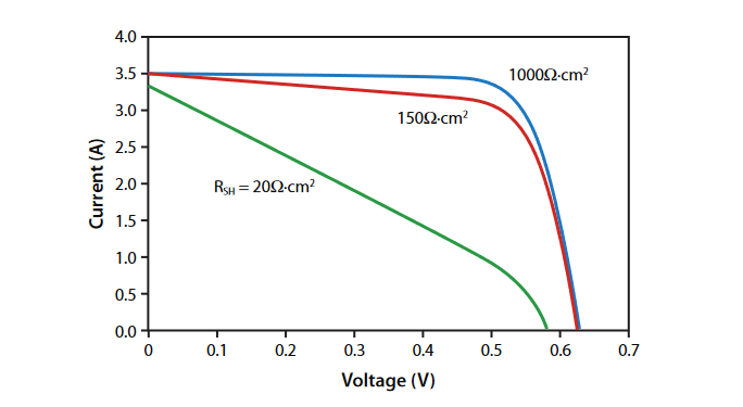
Any decrease in RSHUNT creates a more attractive leakage path, which allows more of the cell current and power to be lost. This can be caused by leakage in the interconnect, but it is more often an effect of the intrinsic cell design. As the plot shows, this percentage drop in current looks like a change in slope on what should be the flat part of the I-V curve.
Series resistance (RSERIES): An increase in series resistance will cause a cell's efficiency to decrease. Intuitively, one can think of RSERIES as taking voltage from the load as the diode turns on. Given that RSHUNT is much greater than RSERIES, RSERIES doesn't normally affect the amount of current being delivered but directly takes voltage from the load as it appears in series. As RSERIES increases, cell efficiency decreases.
Conversion efficiency: The percentage of power converted (from absorbed light to electrical energy) and collected when a solar cell is connected to an electrical circuit. This term is calculated by dividing Pmax by the input light irradiance (E, in W/m2, measured under standard test conditions) multiplied by the surface area of the solar cell (AC, in m2).
Doping density (N): Doping density is an important property of any doped semiconductor material. Taken together, information on doping density and resistivity provide valuable information about the quality of a material. By adding assumptions about the consistency of the fabrication process, it's possible to infer the electron mobility within the material.Understanding the mobility, doping density, and resistivity and eventually the changes over operating temperatures can help you to refine your process. In general, resistivity should decrease as dopant density increases and mobility should decrease as dopant density increases.Usually, to achieve optimal behavior as part of a fabricated solar cell, material researchers want to find a balance between sufficiently low resistivity and sufficiently high mobility, which are both seen as important to cell operation.
Cell resistivity (van der Pauw resistivity or surface resistivity): There are two common methods for resistivity measurements on semiconductor materials: four-point collinear probe measurements and van der Pauw resistivity measurements. These techniques can be used to find the surface resistivity and conductivity of the material itself, which are important in optimizing fabrication techniques.
Defect density: Defect density is a measure of defects (electrons or holes) in the active region of the semiconductor material. Drive Level Capacitance Profiling (DLCP) is a new measurement technique used to characterize this material property. Understanding when defects appear in a semiconductor material is important to refining a fabrication process.
Current density: A measurement used in comparing the outputs of cells of different sizes.Current density refers to the amps of current produced per square centimeter of cell area.
Quantum efficiency (QE): The quantum efficiency of a solar cell is a measure of efficiency over wavelength. Changes in quantum efficiency might indicate different processes occurring at the junction that would affect the cell’s efficiency. In essence, QE is a measure of the likelihood of an incoming photon (of a certain wavelength) resulting in an electron flowing to the load. QE is typically measured by using a monochromator and illuminating the cell with a single wavelength (or small set of wavelengths) at a time of known intensity, performing an I-V sweep and calculating efficiency at that wavelength. The test would be repeated at multiple wavelengths or sets of wavelengths.
Find more valuable resources at TEK.COM
Copyright © Tektronix. All rights reserved. Tektronix products are covered by U.S. and foreign patents, issued and pending. Information in this publication supersedes that in all previously published material. Specification and price change privileges reserved. TEKTRONIX and TEK are registered trademarks of Tektronix, Inc. All other trade names referenced are the service marks, trademarks or registered trademarks of their respective companies.
No.3067 12/07.09

