Hall effect measurements have been valuable tools for material characterization since Edwin Hall discovered the phenomenon in 1879. Essentially, the Hall effect can be observed when the combination of a magnetic field through a sample and a current along the length of the sample creates an electrical current perpendicular to both the magnetic field and the current, which in turn creates a transverse voltage that is perpendicular to both the magnetic field and the current (see Figure 1). The underlying principle is the Lorentz force, that is,the force on a point charge due to electromagnetic fields. The "right hand rule" we all learned in our introductory physics classes allows us to determine the direction of the force on a charge carrier based on its direction of motion and the direction of the applied magnetic field.
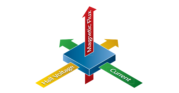
This white paper addresses how Hall effect measurements are used in materials characterization, trends in the semiconductor industry that drive the need for making these measurements, and factors to consider when selecting measurement instrumentation.
Who Needs to Measure Hall Effect?
Hall effect measurements are used in many phases of the electronics industry, from basic materials research and device development to device manufacturing. Users include integrated circuit producers, particularly their technology and their process development groups.Crystal manufacturers also use this measurement technique, as do researchers in universityand industry-based labs. For example, nanotechnology researchers studying graphene,a single-atom-thick, crystalline form of carbon, determined recently that the material demonstrated the quantum Hall effect; therefore, the electrons flowed through the crystal with relatavistic effects.
A Hall effect measurement system can actually be used to determine quite a few material parameters, but the primary one is the Hall voltage (VH). Other important parameters such as carrier mobility, carrier concentration (n), Hall coefficient (RH), resistivity, magnetoresistance (R ), and the conductivity type (N or P) are all derived from the Hall voltage measurement.With the addition of some other instruments, I-V characterization curves can be created with a similar test setup.
Hall effect measurements are useful for characterizing virtually every material used in producing semiconductors, such as silicon (Si) and germanium (Ge), as well as most compound semiconductor materials, including silicon-germanium (SiGe), silicon-carbide (SiC), gallium arsenide (GaAs), aluminum gallium arsenide (AlGaAs), indium arsenide (InAs), indium gallium arsenide (InGaAs), indium phosphide (InP), cadmium telluride (CdTe), and mercury cadmium telluride (HgCdTe). They’re often used in characterizing thin films of these materials for solar cells/photovoltaics, as well as organic semiconductors and nano-materials like graphene. They are equally useful for characterizing both low resistance materials (metals, transparent oxides, highly doped semiconductor materials, high temperature superconductors, dilute magnetic semiconductors, and GMR/TMR materials used in disk drives) and high resistance semiconductor materials, including semi-insulating GaAs, gallium nitride (GaN), and cadmium telluride (CdTe).
Growing Interest in the Use of Hall Effect Measurements
Hall effect measurements were first routinely used in the semiconductor industry more than two decades ago, when scientists and researchers needed tools for characterizing bulk silicon materials. However, once the bulk mobility of silicon was well understood, Hall effect measurements were no longer considered critical. But today's semiconductor materials are not just silicon-manufacturers often add germanium to silicon in the strain lattice to get higher mobility. Moreover, modern semiconductor materials are no longer bulk materials-they're often in the form of thin films, such as those used in copper indium gallium diselenide (CIGS) and CdTe solar cells. As a result, IC manufacturers now have to go back to determining carrier concentration and carrier mobility independently, applications for which Hall effect measurements are ideal. Hall effect measurements can also be used for characterizing novel storage devices that employ quantized Hall effect, magnetoresistance profiling, etc.
Another factor driving the growing interest in the Hall effect is related to how much current a device can handle. If device designers can maximize current flow, the devices they create can operate at lower power levels, switch faster, and have higher bandwidth. Several factors affect the magnitude of this current. The current is directly proportional to the carrier concentration, carrier mobility, the applied voltage and the cross-sectional area; it is inversely proportional to the sample length.
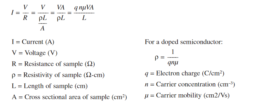
Theoretically, there are several alternative approaches to increasing the level of current flow through a device, but all but one of them has significant disadvantages:
- Increasing voltage (V): Increasing the voltage through a device involves consuming additional power and generating heat. Today, however, the trend is heavily in the direction of mobiles devices like smartphoness, netbooks, tablet computers, and e-readers,in which long battery life is highly desirable, which makes increasing the voltage counterproductive
- Increasing the number of electrons (n): There's a limit to how much a semiconductor can be doped before it saturates or reaches its solid solubility limit, so materials scientists can only go so far in increasing the number of electrons.
- Increasing the cross-sectional area of the sample (A): Again, increasing device area conflicts with the consumer demand for light, compact handheld devices.
- Increasing the mobility of electrons or carriers: This is the optimum approach to maximizing current flow through a device. For materials scientists and solid-state physicists, Hall effect measurements are key to characterizing combinations of materials with high carrier mobilities.
Measuring Mobility Using Hall Effect Techniques
The first step in determining carrier mobility is to measure the Hall voltage (VH) by forcing both a magnetic field perpendicular to the sample and a current through the sample. The combination of the current flow (I) and the magnetic field (B) causes a transverse current. The resulting potential (VH) is measured across the device. Accurate measurements of both the sample thickness (t) and its resistivity (ρ) are also required. The resistivity can be determined using either a four-point probe or van der Pauw measurement technique. With just these five parameters (B, I, VH, t, and resistivity), the Hall mobility can be calculated using this formula:
| µH = | |VHt| |
| BIρ |
Because Hall voltages are typically quite small (millivolts or less), as is the measured van der Pauw resistivity, the right measurement and averaging techniques are critical to obtaining accurate mobility results when using this formula.
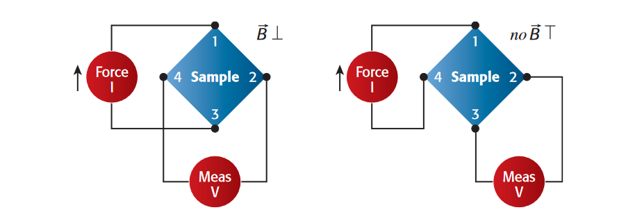
Figure 3 illustrates the measurement configurations for both the Hall effect voltage and the van der Pauw resistivity measurement. Although these measurement configurations are very similar in as much as both use four contacts and both measurements involve forcing a current and measuring a voltage, in the Hall effect measurement, the current is forced on opposite nodes of the sample and then the voltage is measured on the other opposite nodes so the force and the measure contact points are interlaced and the voltage for semiconductors is typically around KT/q, which is about 25 millivolts. It can also be much lower. In contrast, for van der Pauw resistivity measurements, the current is forced on adjacent nodes and then the voltage is measured on opposing adjacent nodes so everything that is being forced and measured are on nearest pins; in that case, the voltages can be well above 20 millivolts. The voltages can be anywhere from millivolts for low resistivity materials to 100 volts for very high resistivity insulating materials. The other major differentiator is that there is no magnetic field being applied in the van der Pauw measurement, whereas for the Hall effect measurement, a transverse magnetic field is applied.
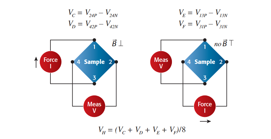
To obtain results with high confidence, the recommended technique involves a combination of reversing source current polarity, sourcing on additional terminals, and reversing the direction of the magnetic field. Eight Hall effect (Figure 4) and eight van der Pauw (Figure 5) measurements are performed. If the voltage readings within each measurement differ substantially, it’s advisable the recheck the test setup to look for potential sources of error.
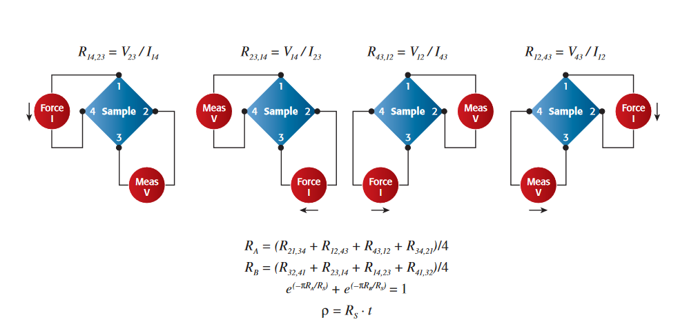
A basic Hall effect measurement configuration will likely include the following components and optional extras:
- A constant-current source of a magnitude that’s dependent on the sample's resistance.For low resistivity material samples, the source must be able to output from milliamps to amps of current. For samples such as semi-insulating GaAs, which may have a resistivity in the neighborhood of 107 ohm·cm, a sourcing range as low as 1nA will be needed. For high resistivity samples (such as intrinsic semiconductors), the constantcurrent source may have to be able to go as low as 1nA, but a source capable of producing current from 10 microamps to 100 milliamps will suffice.
- A high input impedance voltmeter. Depending on the level of material resistivity under test, the voltmeter used must be able to make accurate measurements anywhere from 1 microvolt to 100V. High resistivity materials may require ultra-high input Z or differential measurements.
- A permanent magnet or an electromagnet. These are typically available with ranges from 500 to 5000 gauss. An electromagnet will also require a power supply to drive it.
- A sample holder.
- Optional equipment. A switch matrix is generally included to eliminate the need for manual connections/disconnections between probe contacts; it may also make it possible to test multiple samples at once. A switch matrix is definitely required if the sample is being held in a liquid nitrogen dewar for temperature studies.
Hall mobility is highly dependent on sample temperature, so it's often desirable to monitor this temperature, particularly if the application involves repeating measurements each time the sample’s temperature is adjusted. Many test configurations include a temperature-measuring probe; for high accuracy work, the probe’s resolution should be about 0.1° Celsius. A prober chuck that can either heat or cool the sample and a temperature controller are generally necessary for on-wafer measurements when doing temperature studies. A cryostat is necessary to hold the sample in the liquid nitrogen bath for low temperature studies.
For making on-wafer measurements of numerous devices, a prober with a manipulator and probe tips will likely be essential.
Although someone working in a lab at a crystal manufacturer, for example, will most likely only want to do Hall effect measurements, someone setting up a multi-purpose characterization lab will likely need other types of measurements, too, such as collinear resistivity, full I-V sweeps, C-V measurements, transient response studies, and other measurements. Therefore, when selecting equipment for Hall effect measurement,it's wise to consider the additional measurements that may be required to address a particular material characterization challenge.
Matching the Configuration to the Hall Effect Application
The most appropriate Hall effect measurement configuration for a particular application will be based in large part on the sample's total resistance as measured by the electrical test equipment. This total resistance is the sum of the sample resistance and the contact resistance,that is, the resistance between the sample and the electrical contacts to it.
The sample resistance depends on the sample's intrinsic resistivity, which is expressed in units of ohm-centimeters (ohm·cm), and its thickness. For a square sample, the sample resistance would be calculated as the sample’s resistivity divided by its thickness.
For a silicon sample, the contact resistance is typically about 300 times the sample resistance. In contrast, GaAs, one of the wide bandgap materials, has a contact resistance roughly 1,000 times its sample resistance. Therefore, as a result of this high contact resistance,a low resistance sample of GaAs may have far higher total resistance than a mid-range resistance silicon sample. Also, the total resistance of your configuration can be much higher than just the resistance of the sample. The total configuration of your sample configuration will determine what the optimal instrument configuration needs to be.
Before selecting Hall effect test equipment, it’s advisable to consult ASTM F76-08: Standard Test Methods for Measuring Resistivity and Hall Coefficient and Determining Hall Mobility in Single-Crystal Semiconductors
Electrical test setups for Hall effect measurements are typically intended for one of four resistance ranges:
- Mid-range resistance : range of test equipment is typically suited for characterizing materials such as nominally doped silicon or germanium (approximately 1015cm-3),silicon-based photovoltaic materials, pseudomorphic high electron mobility transistors (pHEMTs), and indium tin oxide (ITO).
- Low resistance : Low resistance samples are often metals, highly doped silicon or germanium (greater than 1017cm-3) or a combination of silicon and germanium,superconductive materials, or materials intended for the production of giant magnetoresistance and tunnel magnetoresistance (GMR/TMR) heads. New nanomaterials such as graphene can fall into this category.
- Low-to-high (wide range) resistance : This wide range of resistance is typical of thinfilm photovoltaic materials like CIGS, CdTe, and HgCdTe.
- Mid-to-super-high resistance : This level of resistance is common with semi-insulating silicon and many of the wide bandgap or compound semiconductors.
Configuration Example: Low-to-High Resistance Range
Each of these resistance ranges has differing measurement requirements and the type and number of components of the systems needed to test them can vary significantly. To illustrate the configuration process, here's an example of a configuration appropriate for the widest range of sample resistances, from 1 micro-ohm to 1 terra-ohm. A configuration of this type would be most appropriate for those characterizing thin-film photovoltaic materials, those who are studying the effects of doping concentration on an intrinsic semiconductor, or those studying the effects of doping polymers with increasing amounts of carbon nanotubes.This system configuration (see Figure 6) employs Keithley's special matrix switching card optimized for Hall effect measurements, the Model 7065, housed in a Model 7001 Switch Mainframe. This card buffers test signals from the sample to the measurement instrumentation and switches current from the current source to the sample. The Model 7065 card offers the advantage of unity gain buffers that can be switched in and out to allow the measurement of high resistances by buffering the sample resistance from the meter.
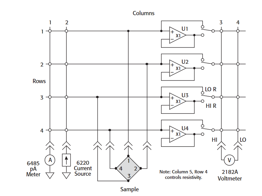
The test setup also includes the Model 6485 Picoammeter, the Model 6220 DC Current Source, and the Model 2182A Nanovoltmeter. The Model 6485 Picoammeter is included to measure leakage currents so they can either be subtracted out or monitored to make sure they aren't impacting the high resistance measurement. The Model 6220 and the Model 2182A are designed to work together seamlessly, using a delta mode technique to synchronize their operation and optimize their performance. Essentially, the delta mode automatically triggers the current source to alternate the signal polarity, then triggers a nanovoltmeter reading at each polarity, cancelling out both constant and drifting thermoelectric offsets, and ensuring the results reflect the true value of the voltage. Once the Model 6220 and the Model 2182A are connected properly, all it takes to start a test is pressing the current source's Delta button and then the Trigger button. The Model 2182A also provides a second channel of voltage measurement capability, which is useful for monitoring the temperature of the sample.Although the Model 6220 serves as the constant current source in the configuration shown, substituting the Model 6221 AC+DC Current Source, which has a built-in arbitrary waveform generator, has the advantage of allowing users to make AC Hall effect measurements. For applications for which it acceptable to trade off the low resistance capability of the system shown to reduce the system cost (i.e., to provide just mid-range to high resistance capability), a Model 2000 Digital Multimeter can be substituted for the Model 2182A Nanovoltmeter.
Enhancing Hall Effect Measurement Confidence
Incorporating a number of good measurement practices into the design of a Hall effect system will increase the likelihood of getting high integrity measurements on high resistivity materials:
- Always incorporate electrostatic shielding into the system's design to minimize electrical interference : Electrostatic coupling or interference occurs when an external electric field impinges upon the circuit under test. At low impedance levels, the effects of the interference usually aren't noticeable because any charge that is developed dissipates rapidly. However, high resistance materials don't allow the charge to decay quickly, which may result in unstable measurements. Either DC or AC electrostatic fields may be responsible for these erroneous readings, so always use electrostatic shielding to minimize their effects. As much as practicable, shield the sample being tested and all sensitive measurement circuitry, connect the shield to the low terminal of the test system, and always use shielded cabling. The easiest type of shield to make is a simple metal box or meshed screen that encloses the test circuit. Shielded boxes are also available commercially. For further details on shielding techniques, consult Section 2 of Keithley's Low Level Measurements Handbook.
- Ensure the test system is properly grounded : When there are two or more connections to earth, such as when source and measuring instruments are both connected to a common ground bus, a group loop is formed, which can introduce noise and error voltages. A voltage (VG) between the source and instrument grounds will cause a current (I) to flow around the loop. This current will create an unwanted voltage in series with the source voltage. Ground loops can occur when a number of instruments are plugged into power strips on different instrument racks. Frequently, there is a small difference in potential between the ground points, which can cause large currents to circulate and create unexpected voltage drops. Prevent ground loops from forming by grounding all equipment in the test system at a single point by using isolated power sources and instruments, then establishing a single, good earth-ground point for the entire system.Avoid connecting sensitive instruments to the same ground system used by other instruments, machinery, or other high power equipment.
- Use guarding to reduce the effects of leakage current in the system : This includes the use of a guarded current source, guarded voltmeters, and triaxial rather than coaxial cables.
- Be sure to allow sufficient settling time before making measurements. If you are measuring a high resistance sample, the capacitance in the cabling combined with the high resistance sample creates a large RC time constant, which will cause substantial time delays for voltage levels to reach stable values. To determine the amount of delay time before a voltage level stabilizes, monitor the voltage as a function of time. For example, the voltage on a sample with 1012Ω resistance may not settle for 20 seconds
- Regularly verify the system's performance. The simplest way to do this is to build a test structure using four resistors of equal value that are similar in magnitude to the resistance of the sample under test and use this as a basis for comparison. It's also possible to have NIST characterize a "golden sample" so you can compare your measurement results with theirs.
- Minimize sources of thermoelectric voltages. Whenever possible, use the same materials in all connections, such as all copper connections and copper wire. Reverse the current source's polarity and average the readings to eliminate EMF errors (as the Model 6220/Model 2182A's delta mode allows). Always allow the test equipment to warm up and reach thermal equilibrium before the start of testing, and minimize temperature gradients across the sample.
Conclusion
As the need to characterize high mobility materials becomes increasingly critical, the ability to make accurate Hall effect measurements becomes increasingly important. For more information and additional system schematics for Hall effect systems, view the Keithley online webinar, "Hall Effect Measurement Fundamentals," available on Keithley's website at http://www.keithley.com/events/semconfs/webseminars.
Find more valuable resources at TEK.COM
Copyright © Tektronix. All rights reserved. Tektronix products are covered by U.S. and foreign patents, issued and pending. Information in this publication supersedes that in all previously published material. Specification and price change privileges reserved. TEKTRONIX and TEK are registered trademarks of Tektronix, Inc. All other trade names referenced are the service marks, trademarks or registered trademarks of their respective companies.
No.3111 01.26.11

