High brightness light emitting diodes (HBLEDs) combine high output and high efficiency with long lifetimes. Manufacturers are developing devices that offer higher luminous flux, longer lifetimes, greater chromaticity, and more lumens per watt. Ensuring their performance and reliability demands accurate, cost-effective testing at every phase of production.
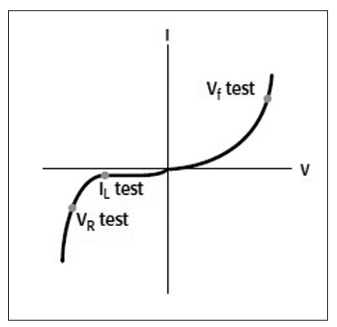
The electrical I-V curve of a typical diode is illustrated in Figure 1. Although a complete test sequence could include hundreds of points, a limited sample is generally sufficient to probe for the figures of merit. Many HBLED tests require sourcing a known current and measuring the resulting voltage or vice-versa. Instruments that combine synchronized sourcing and measurement can speed system setup and enhance throughput. Testing can be done at the die level (both wafer and package), or the module / subassembly level. At the module/subassembly level, HBLEDs are connected in series and/or parallel; therefore, higher currents are typically involved, sometimes up to 50A or more, depending on the application. Some die-level testing can be in the range of 5 to 10 amps, depending on die size.

Forward Voltage Test
Understanding how new building-block materials like graphene, carbon nanotubes, silicon nanowires, or quantum dots will perform in the electronic devices of tomorrow demands instrumentation that can characterize resistance, resistivity, mobility, and conductivity over wide ranges. Often, this requires the measurement of very small currents and voltages. The ability to create accurate and repeatable measurements at the nanoscale level is critical to engineers seeking to develop and commercialize these next generation materials.
Optical Tests
Forward current biasing is also used for optical tests because current flow is closely related to the amount of light an HBLED emits. A photodiode or integrating sphere can be used to capture the emitted photons to measure optical power. This light is converted to a current that’s measured using an ammeter or one channel of a sourcemeasure unit (SMU).
Reverse Breakdown Voltage Test
A negative bias current applied to an HBLED allows probing for its reverse breakdown voltage (VR). The test current should be set to a level where the measured voltage value no longer increases significantly when current is increased slightly. At higher voltages, large increases in reverse bias current produce insignificant changes in reverse voltage. The VR test is performed by sourcing a low-level reverse bias current for a specified time, then measuring the voltage drop across the HBLED. Results are typically in the tens of volts.
Leakage Current Testing
Moderate voltages are normally used to measure the current that leaks across an HBLED when a reverse voltage less than breakdown is applied (IL). In production testing, it's common practice to ensure only that leakage doesn’t exceed a specified threshold.
Boosting HBLED Production Test Throughput
Once, a PC controlled all aspects of HBLED production test. In other words, in each element of a test sequence, the sources and instruments had to be configured for each test, perform the desired action, and then return the data to the PC. The controlling PC evalsuated the pass/fail criteria and determined where to bin the DUT. Significant time was consumed by passing commands from the PC and results back to it.
The latest generation of smart instruments, including Keithley’s new High Power 2651A System SourceMeter, boost throughput substantially by minimizing communications traffic. The majority of the test sequence is embedded in the instrument in a Test Script Processor (TSP®), a test sequence engine that allows control of the test sequence, with internal pass/fail criteria, calculations, and control of digital I/O. A TSP stores a user-defined test sequence in memory and executes it on command, reducing set-up and configuration time for each step in the sequence.
LED Test System for a Single Device
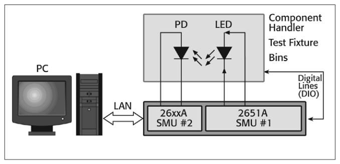
The component handler transports the individual HBLED (or group of HBLEDs) to a test fixture, which is shielded from ambient light and houses a photodetector (PD) for light measurements. Two SMUs are used: SMU #1 supplies the test signal to the HBLED and measures its electrical response; SMU #2 monitors the photodiode during optical measurements.
The test sequence is programmed to begin using a digital line from the component handler that serves as a "start of test" (SOT) signal. After the instrument detects this signal, the test sequence begins. Once completed, a digital line to flag "measurement complete" is set for the component handler. In addition, the instrument's built-in intelligence performs all pass/fail operations and sends a digital command through the instrument's digital I/O port to the component handler to bin the HBLED based on the pass/fail criteria. Then, two actions can be programmed to take place simultaneously: data is transferred to the PC for statistical process control and a new DUT moves into the test fixture.


Testing Multiple HBLED Devices
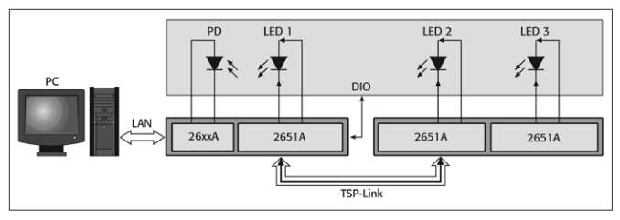
Applications such as burn-in involve measuring multiple parts simultaneously.
Minimizing HBLED Testing Error
Junction self-heating is among the most significant error sources in HBLED production test. As the junction heats over time, the voltage drops or, more importantly, the leakage current increases, so it's crucial to minimize test times. Smart instruments can simplify configuring the device soak time (which allows any circuit capacitance to settle before the measurement begins), as well as the integration time (which defines how long the A-to-D converter acquires the input signal). New SMU instruments, such as the Keithley 2651A, have digitizing A-to-D converters, which can sample at speeds up to one microsecond per point, which is up to 50 times faster than high-performance integrating A-to-D converters. These higher measurement speeds further improve overall test times.
The use of pulsed measurements minimizes test times and junction self-heating. Modern SMUs with high pulse width resolution ensure precise control over how long power is applied to the device. Pulsed operation also allows these instruments to output current levels well beyond their DC capabilities.
Find more valuable resources at TEK.COM
Copyright © Tektronix. All rights reserved. Tektronix products are covered by U.S. and foreign patents, issued and pending. Information in this publication supersedes that in all previously published material. Specification and price change privileges reserved. TEKTRONIX and TEK are registered trademarks of Tektronix, Inc. All other trade names referenced are the service marks, trademarks or registered trademarks of their respective companies.
No.3125 4.27.11

